Taiwan Semiconductor Manufacturing Company (TSMC) is accelerating engineering and validation work on a next-generation packaging approach known as CoPoS, which moves assembly from circular 12-inch wafers to square 310mm x 310mm panels. According to reporting by DigiTimes, TSMC has established an initial pilot line at VisEra's Longtan facility and plans to run a second pilot at its AP7 site in Chiayi, but industry expectations place mass production no earlier than 2029.
The company is positioning CoPoS as the logical successor to its current CoWoS packaging architecture, which has played a pivotal role in the rollout of large AI accelerators. The panel format is specifically designed to reduce material waste and lower costs as chiplet sizes increase, an economic case that TSMC and its partners are treating as central to the technology's eventual commercialization.
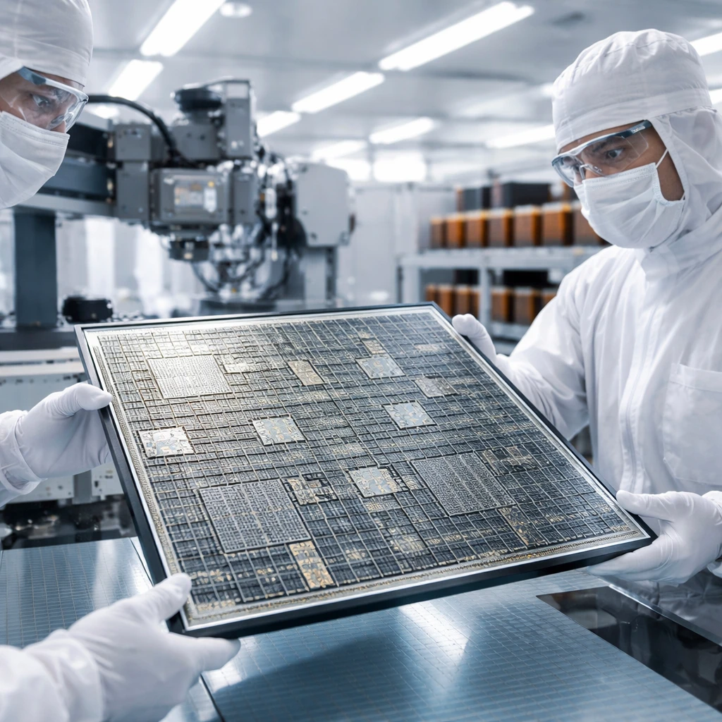
Pilot program and secrecy
TSMC's initial pilot is running at VisEra's Longtan plant, with a follow-up pilot planned for the AP7 facility in Chiayi to continue process validation. DigiTimes characterizes the pilot structure as two-stage, underscoring the volume of engineering work required before scaling to production volumes. The foundry has imposed strict non-disclosure agreements and exclusive-supply clauses on equipment makers, material suppliers, and key component vendors participating in CoPoS development, with cooperation agreements explicitly designed to prevent R&D leakage.
Those contractual controls reflect the program's strategic importance and TSMC's intent to preserve a competitive lead over rivals, including Intel and Samsung, which are reported to be pursuing their own panel-level packaging efforts.
Why square panels?
The economic rationale driving the transition from round wafers to square panels is straightforward. As chip dimensions grow to accommodate larger AI accelerators, the curved edges of circular wafers produce an increasing amount of unusable interposer area. Square panels substantially reduce or eliminate this edge waste, improving material utilization and offering a clear path to lower unit costs for very large chiplets. TSMC is presenting CoPoS as the next stage beyond CoWoS, aiming to capture cost reductions as package sizes scale.
Manufacturing challenges
CoPoS introduces a set of manufacturing challenges considered materially different and, in several respects, greater than those faced with CoWoS. These include the adoption of glass substrates at panel scale, development of large-format redistribution layers, management of low-warpage across broad panel surfaces, and deployment of novel metrology and inspection techniques tailored to panel-sized assemblies. The second pilot at AP7 is intended to address these process and equipment issues as TSMC moves from proof-of-concept to production readiness.
Supplier landscape and domestic sourcing
DigiTimes reports that Taiwanese equipment and materials suppliers are likely to be the immediate beneficiaries of the CoPoS program, since local vendors can more rapidly support the intensive R&D cycles the initiative demands. The foundry's cooperation agreements reportedly include exclusive-supply provisions and require strict confidentiality. An unnamed industry source quoted by DigiTimes suggested Taiwanese suppliers currently demonstrate greater responsiveness than many international competitors, noting that local vendors are often willing to work overtime to meet program needs.
Bill Chiu, chairman of Gudeng Precision, a Taiwanese supplier involved in CoPoS validation, told DigiTimes that "CoPoS will definitely happen," while emphasizing that the effort represents a generational upgrade built on existing process knowledge rather than a clean-sheet design. Chiu added that after technical maturity is achieved, the primary focus will shift to cost optimization, implying that pricing pressure on early CoPoS capacity will come after technical stabilization.
Standards, geopolitics and industry implications
Standardization of panel dimensions remains unresolved. While TSMC's internal format is 310mm x 310mm, other players are reported to be experimenting with different panel sizes. That fragmentation could complicate an industry-wide transition and will need coordination before multi-customer commercial deployment becomes practical.
The concentration of R&D and supplier activity in Taiwan, combined with strict export-adjacent confidentiality controls, heightens the geopolitical significance of the island's semiconductor ecosystem. DigiTimes notes that the program's design and validation with Taiwanese suppliers deepens Taiwan's strategic role at a time when policymakers in Washington and Taipei are focused on preserving technological advantage.
Near-term watch points for investors
- Progress updates from the AP7 pilot line in Chiayi as TSMC advances process validation.
- Any acceleration of competing panel-level programs by Intel or Samsung.
- Disclosure of CoPoS-related supplier relationships in the quarterly reports of Taiwan-listed equipment and materials companies.
- TSMC commentary on packaging capacity in its quarterly results, which would clarify the pace of a transition from CoWoS to panel-level CoPoS.
With a 2029 mass-production target now reflected in market expectations, the technical and commercial sequencing set out by TSMC and its suppliers will determine how quickly AI chip customers such as large hyperscale designers can migrate to panel-level packaging. That sequencing will also shape near-term cost dynamics across the AI semiconductor supply chain.