Applied Materials Inc reported a notable market reaction after announcing a set of six new systems developed for DRAM manufacturing and advanced packaging workflows, sending its shares up 7.1% on Thursday.
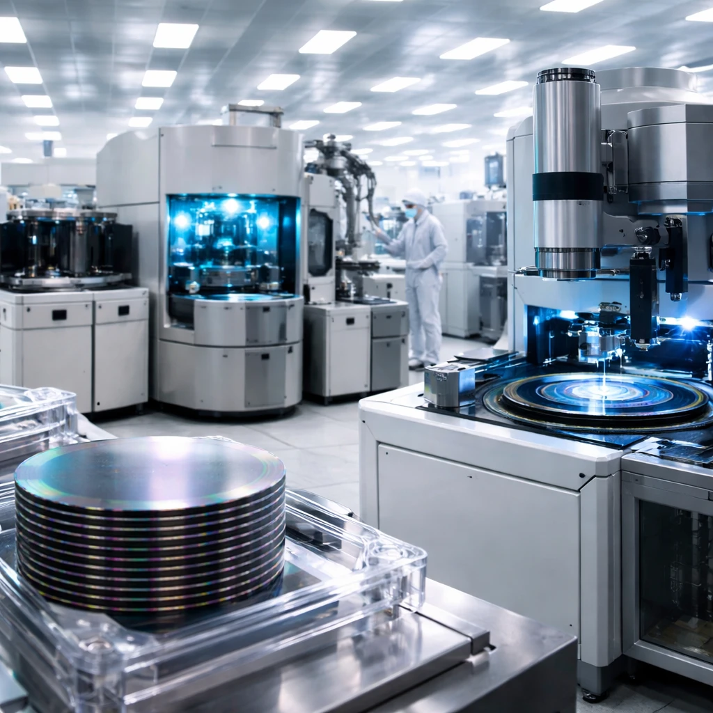
The systems were revealed on June 25, 2026 and are aimed at accelerating production for 3D chip architectures that underpin next-generation artificial intelligence workloads. Applied Materials framed the product introductions as a response to a so-called "memory wall" in AI computing - a situation where data movement requirements are outpacing gains in bandwidth and energy efficiency.
The new lineup includes an updated Centura Prime Epi system that applies logic-class epitaxy methods to DRAM production. According to the company, the enhanced Centura Prime Epi grows doped silicon germanium and silicon phosphorous in transistor regions. Applied Materials says this enables faster and more power-efficient DRAM operation targeted at high bandwidth memory and next-generation DDR applications. The updated system also features a reduced footprint, about 20% smaller than previous versions.
For advanced packaging processes the company introduced three systems addressing critical manufacturing steps:
- Opta Quad CMP - a chemical mechanical planarization platform that incorporates real-time monitoring and dynamic adjustments to improve uniformity in planarization.
- Nokota VMax 2 ECD - an electrochemical copper deposition system intended for through-silicon vias and microbump formation.
- Producer Avila 2 PECVD - a plasma-enhanced chemical vapor deposition tool that deposits stress-balanced dielectric films to stabilize ultra-thin DRAM dies used in high-layer-count HBM designs.
Applied Materials also added two electron-beam systems focused on process control in packaging fabs. The VeritySEM 7AP is described as providing critical dimension metrology with sub-10nm sensitivity, while the SEMVision G7AP targets high-resolution defect analysis across a range of substrate types. Both instruments are designed to address the specific difficulties of measuring features on thick, warped substrates common in HBM and chiplet architectures.
The equipment announcement coincided with broader gains in memory-linked equities after Micron reported strong earnings. The piece of industry news helped lift memory-related stocks during Thursday trading; the article notes that Micron and Sandisk shares were up more than 12% at the time of reporting, and that the Roundhill Memory ETF was trading nearly 8% higher.
Applied Materials' product introductions span epitaxy, planarization, copper deposition, dielectric deposition and electron-beam metrology - a collection designed to address both device-level DRAM scaling and the packaging challenges that accompany dense, multi-layer memory stacks.
Market context
The stock move followed the company's product announcement and came amid a memory sector rally tied to Micron's earnings. The new systems are positioned to serve demand for 3D memory architectures and advanced packaging processes that developers say are critical for AI workloads.