Stock Markets March 31, 2026

TSMC Schedules 3-nanometre Equipment Installation and Mass Production in Japan for 2028

Second Japanese fabrication site to target 15,000 12-inch wafers per month using advanced 3nm processes under revised plan

By Hana Yamamoto TSM
TSMC Schedules 3-nanometre Equipment Installation and Mass Production in Japan for 2028
TSM

Taiwan Semiconductor Manufacturing Co. (TSMC) plans to begin equipment installation and mass production of 3-nanometre wafers at its second fabrication plant in Japan in 2028, according to a Taiwanese government filing. The revised plan sets the second plant's monthly capacity at 15,000 12-inch wafers using advanced 3-nanometre process technology. This marks a shift from earlier plans focusing on less-advanced nodes and follows prior investment guidance that total spending for both Japanese fabs would exceed $20 billion.

Key Points

  • TSMC plans to begin equipment installation and mass production of 3-nanometre wafers at its second Japan fab in 2028, per a Taiwanese government filing.
  • The revised plan assigns the second plant a monthly capacity of 15,000 12-inch wafers using advanced 3-nanometre process technology, while earlier Japan plans focused on less-advanced nodes.
  • TSMC previously said total investment for the first and second Japanese fabs would exceed $20 billion with combined monthly capacity of 100,000 12-inch wafers across 40, 22/28, 12/16 and 6/7-nanometre technologies; a Japanese report placed second-fab investment near $17 billion, which TSMC has not confirmed.

TSMC intends to commence equipment installation and move to volume production of chips using its 3-nanometre process at the company's second fabrication facility in Japan in 2028, according to a Taiwanese government filing filed late on Tuesday. The timeline and production target were outlined in the filing and reflect an updated plan for the site.

In February, TSMC's chief executive CC Wei told Japan's Prime Minister Sanae Takaichi that the company planned to mass-produce advanced 3-nanometre chips at the second Japanese fab. That statement is consistent with the details contained in the more recent government filing.

Under the revised blueprint documented in the filing, the second plant in Japan is slated to reach a monthly output of 15,000 12-inch wafers manufactured on the advanced 3-nanometre process technology. The filing stated this capacity figure explicitly.

TSMC's earlier plans for its Japanese operations centered on less-advanced nodes. In 2024, the company said total investment across its first and second Japanese fabs would exceed $20 billion. At that time, TSMC reported a combined monthly capacity goal of 100,000 12-inch wafers employing less-advanced process technologies, specifically 40, 22/28, 12/16 and 6/7-nanometre nodes.

Japanese media reports in February, citing Yomiuri, indicated that investment for the second fabrication plant could be approximately $17 billion. TSMC has not confirmed that figure and declined to comment on the reported investment amount, according to available information.

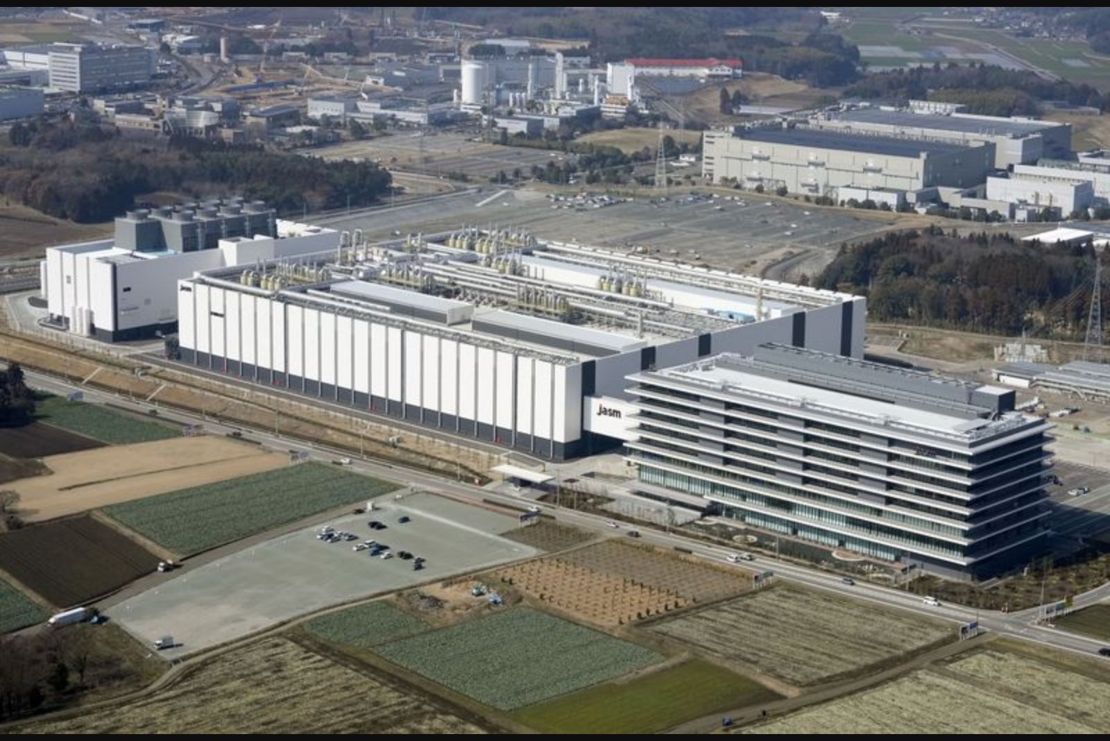
The company's first fabrication plant in Japan began volume production in late 2024. The Japan unit, established in 2021 as Japan Advanced Semiconductor Manufacturing, was formed with support from Sony Semiconductor Solutions Corporation. Later, Japan's DENSO Corporation and Toyota Motor Corporation joined as minority investors in the unit.

Additional commentary and investment tools referenced TSM in a separate promotional segment. That segment described ProPicks AI's evaluation of TSM alongside other companies using financial metrics, and it listed past winners identified by that service. The promotional content noted that ProPicks AI generates stock ideas based on fundamentals, momentum, and valuation and invited readers to check whether TSM is featured in any strategies.


Contextual note: The reporting above is based strictly on details provided in the Taiwanese government filing and related statements cited in February; no additional projections or external analysis have been introduced.

Risks

  • Investment uncertainty - a Japanese report cited an approximate $17 billion investment for the second fab, but TSMC has not disclosed or commented on that figure; this creates ambiguity around capital deployment and financial planning for the project. (Impacted sectors: capital markets, semiconductor supply chain)
  • Timeline and execution risk - the plan sets a 2028 start for equipment installation and mass production of 3-nanometre wafers, but the filing provides the target without further operational detail; this leaves schedule execution and ramp-up subject to uncertainty. (Impacted sectors: semiconductor manufacturing, electronics)
  • Capacity mix and technology focus - TSMC's revised emphasis on advanced 3-nanometre production at the second Japanese plant represents a change from earlier plans emphasizing less-advanced nodes, which could affect supply allocation across product lines and customers. (Impacted sectors: consumer electronics, automotive semiconductors)

More from Stock Markets

Grab and WeRide Begin Robotaxi Service in Singapore Residential Estate Apr 1, 2026 TSMC to Manufacture 3-nm Chips in Japan Starting 2028, Filing Shows Apr 1, 2026 Samsung, SK Hynix Rally as Tech Stocks Rebound After Heavy March Losses Apr 1, 2026 Asian Markets Rally as Trump Signals Possible End to Iran Conflict; South Korea Leads Gains Mar 31, 2026 Asia Stocks Rally as Hopes Grow for Near-Term De-escalation in Iran Conflict Mar 31, 2026